Hardware & Assembly
xxxx xx xx
The following are notes from my Hardware and Assembly class back in univerity.
Contents
- Hardware Architecture
- Logic
- Cominational Circuits
- Sequential Circuits
- Busses & Registers
- Memory Unit Sizes
- Microprocessors
- Assembly Language
- Storing data in binary
- Negative Numbers
- Floating Point Numbers
- Memory &camp; Cache
- Virtual Memory
- Least Recently Used
- Glossary
Hardware Architecture
A "Computer" can be thought of as a collection of various hardware components that all work together. The processor, memory, I/O, video card, ethernet port, storage devices, are all hardware components. This course is about the organization of these components and how to handle signals and interface between them.
Why binary? 1s and 0s? Well, we need a way to work with data and so we need a way to represent all kinds of data (graphics, books, movies, etc.) in some manner of electricity. Computers run on electricity after all. The most obvious answer is using voltage. High voltage versus low voltage.
So how do we convert "data" to binary? It's most obvious if we have a number. Say for example we want a computer to remember we have $24. Here, we just convert the number "24" into binary, "24" into 1's and 0s... Okay but how do we do that?
Decimal numbers are "base 10" meaning there are 10 unique symbols (0, 1, 2, 3, 4, 5, 6, 7, 8, 9) to represent any number. To make bigger numbers, we add more digits to the left and keep counting up (10, 11, 12, 13, 14, 15, 16, 17, 18, 19, 20, 21...).
Binary numbers are "base 2" meaning there are only 2 unique symbols (0, 1). To represent any number in binary, just add more digits to the left and keep counting up (0, 1, 10, 11, 100, 101, 110, 111, 1000) or (0, 1, 2, 3, 4, 5, 6, 7, 8 in decimal).
And this is where the term Bit comes from! A bit is a binary digit. For a wide variety of reasons, hardware operates on groupings of 8 bits. A byte is 8 bits or 8 binary digits. The biggest decimal number a byte can be is 11111111 or 255 decimal.
So now we have a small problem of displaying and reading binary data. Listing out A TON of 1s and 0s is impossible to read by the eye. 110011011111111110010111 is 13,500,311 decimal. And going from 13,500,311 to binary is a huge headache to compute by hand. This is getting out of hand quickly, so what if we use a Number System whose base makes it much easier to read binary and also split binary data up into groupings of 8?
Hexadecimal is base-16 so it uses the symbols (0, 1, 2, 3, 4, 5, 6, 7, 8, 9, A, B, C, D, E, F) to represent decimal numbers 0 through 15. In binary, these would be numbers 0 through 1111 (4 bits). Thus, 2 hexadecimal digits can describe a full byte in a nice little succinct package. Our number earlier can be written in hex as CDFF97. To convert to binary, just take each hex digit and convert it to a 4-bit binary pattern. C (12 decimal) becomes 1100, D becomes 1101, F becomes 1111, and so on.
In short, hexadecimal makes it much easier to read and write binary numbers by hand which we will do surprisingly often.
Additionally, when data is stored in memory (hard drive, RAM, etc.) each byte is given a unique Memory Address. Think of this just like a normal mailing address where your data is located at. If you ever want to get your data back, just go to the address it was saved at and read it. Addresses are always written in hexadecimal.
Logic
So we've got 1s and 0s. Now it's time to use these to make things happen. We can do this by comparing two bits to each-other and producing some sort of output result bit based on that comparison. For example, if we have two bits A and B. We can compare A and B in a variety of ways: are they both 1? At least one of them is 1? Both are 0? A is 1 but B is 0? These are called Logic comparisons.
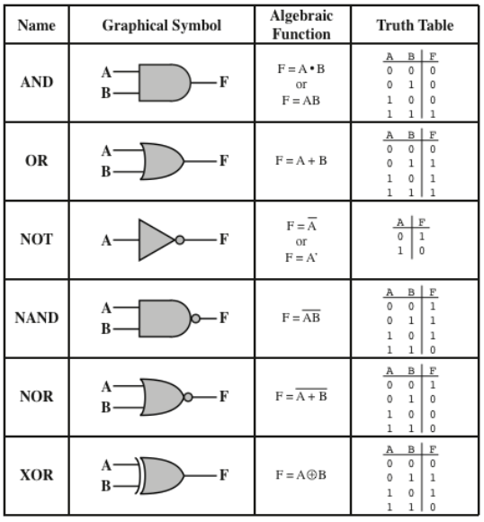
Caption: A table of all basic logic gates (AND, OR, NOT, NAND, NOR, and XOR). The graphical symbol for the gate, its algebraic representation, and a Truth Table showing what the resuting output of the gate is based on the input.
These are all unique possible Logic comparisions with 2 bits. Mostly pay attention to the Name of logic and the Truth Table output.
Notice that the "Algebraic Function" for AND and OR mimics what would happen if you performed that math function on the bits themselves. A * B means bit A times bit B. 1 * 0 is the same as 0 * 0 and 0 * 1 - the result is 0. 1 * 1 is the only way to result in a 1. So, A AND B is the same as multiplying bit A times bit B! This same idea applies for OR but in terms of addition, almost. A OR B means A + B, so 0 + 0 is 0, 1 + 0 = 0 + 1 = 1. The exception is 1 + 1 doesn't result in 2 (binary 10) because that would require outputting 2 bits which we don't do.
Integrated Circuits combine many Logic Gates to perform a more complicated task.
Cominational Circuits
A combinational circuit is an IC of Logic Gates without any memory. They always output the same data when given the same input electrical signal.
Read Only Memory (ROMs) is created using combinational circuits where the input signal is the memory address being accessed. For example, asking for memory address 0x00001234 in a ROM means you're giving an input signal in binary of 0x00001234 and a Combinational Circuit that makes up the ROM is returning a byte as the output where that byte represents the "data stored at that address".
To get all of the memory in a ROM you just move to the next byte, so in our example that's 0x00001235, and repeat until every address is read.
So aside from creating ROMs, what else can Combinational Circuits do?
Imagine you have a stereo, an electric guitar, and an MP3 player hooked up into a speaker system. A Multiplexer is a combinational circuit that allows for one of these input signals to pass through to the speaker based on a separate input signal you're providing via a switch.
Arithmatic Logic Units (which are made of combinational circuits) perform mathematical operations.
Sequential Circuits
These circuits have memory. Their ouptut changs depending on previous signals/data ran through it and the output remains the same until it is told to change.
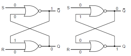
Caption: A circuit diagram of 2 latches. The left Latch has stored a 0, and the right Latch has stored a 1.
Each Latch uses 2 NOR gates. Meaning, it outputs 1 only when both of its inputs are 0. Additionally, the output of each NOR connects as one of the inputs for the other NOR. This means when the Latch is outputing a 0, that 0 data is sent to the upper NOR gate as one of its inputs. The "S" input stands for SET and it tells the Latch to store a 1. The "R" input stands for RESET and tells the latch to store a 0. When both S and R are 0, nothing changes and the Latch continues to output its data. When both S and R are 1, nothing changes and the Latch coninutes to output its data.
I recommend finding a circuit sandbox/toolkit online and making a Latch to see how it works!
Flip-Flop ciruits are a common use of Latches. These are Latches but a Clock circuit feeds the input, meaning the Latch goes back-and-forth between 0 and 1 every time the Clock changes its signal.
Busses & Registers
So we know how to convert data into numbers and convert those into bytes and how those get stored in a computer. Now we need to solve how these various components talk to each other.
Imagine you have 6 different components in your computer that all want to do various things for each other. One program wants to read data from a hard drive, using the processor. Another program wants to store some data to RAM, also using the processor. A third program is driving calls from the graphics card to display a screen, also using the processor. Given what we know about circuits right now, each component would need a hard wire connected directly to the processor to do this! This is wildly unsustainable, we can't have thousands of wires being hard connected to each device.
Busses fix this problem by allowing a single, shared pile of wires from one component to each other. The pile of wires is called the Bus. Only one pair of devices can use the bus at any one moment, but computers work absurdly fast and the bus can happily swap between components many times a second without issue.
Hardware Registers are Flip-Flop circuts (memory) that are specially designed for interfacing between components. They can be used to store data that will be read from another components, or opened to receive data from another component.
Memory Unit Sizes
- A memory unit can have N data lines in, and N data lines out.
- A memory unit can have M address lines.
- This is the actual capacity of the the memory unit.
- Memory is referenced as M x N, or M addresses by N data lines
- This is the number of bits each address stores.
Constructing Memory from Smaller Chips
Larger Memory can be constructed from smaller chips. We just have to make sure that the number of datalines are present as needed and have enough address lines (capacity) as needed.
- Can stack to increase capacity.
- Can stack to increase data lines.
- rows are called pages.
- We need to use extra bits to reference which page we want.
Paging
When large memory is constructed from smaller chips, we need a way to indicate which chips need to send/receive data from the bus. Pages are formed when memory is stacked to increase the number of addresses, not the number of data lines. Paging is used to select just enough chips to make use of all the data lines in the bus.
For example, 128KB x 16 memories built using 32KB x 8 chips. That's 2 chips per page (8 bits x 2 = 16 bits, as needed for the data line) and 21 pages. There are 2 chips per page, so each page is 215 * 2 = 216, and 217 / 216 = 21. This means 17 bits for address selection, 1 bit for page selection, and 1 bit for chip selection. The address will be sent to 2 chips to meet the 16 bit dataline. The page will be used to activate 2 chips via the chip selection.
- Chip Select is used for allowing only certain chips that are a part of a page to output data.
- This outputs fewer data bytes than the bus may allow.
- This is used to allow output to be made up of different addresses on different chips, and eventually end up with just one output.
- Offset Address is the address for each unique reference for each chip
- The page address is used externally, like the offset address.
- The chip select is used internally.
Microprocessors
Microprocessors have an associated memory system and use 2 busses to interact with it. An address bus and a data bus.
Addressability means how the processor will access data, regardless of its data bus size.
- Byte means the processor will access 1 byte at a time.
- Word means the processor will access 2 bytes at a time.
Micro's Memory Unit
- The number of data lines must be filled by the memory unit.
- The outputs of each chip, and the number of data lines needed, determine the number of chips per page.
- Bits for Chip Selection are determined by how the processor is addressable.
- If the processor addresses 1 byte at a time, it needs to activate 1 chip every time.
- If the processor addresses 2 bytes at a time, it needs to activate 2 chips every time.
- The number of bits needed is determined by how many chips there are per page and how many chips need to be accessed at once.
- For byte addressing with 4-chip pages, that's 2 bits to access each 4 chips individually.
- For word addressing with 4-chip pages, that's 1 bit to access each 4 chips, 2 at a time.
- The number of pages you need depends on the number of address lines (total capacity) divided by the memory of the chips per page.
Address Space Partitioning
This is the act of creating address locations for your memory and having each bit mean something. You'll need X bits for chip selection, Y bits for page selection, and then Z bits for offset addressing.
- Every address line in the microprocessor must be used.
- Address Offset is the number of bits needed to address for each chip.
- Bits are set aside for chip select if needed.
- Then set aside bits for page selection.
How do you calculate many chips the memory unit need?
- Chips needed per page to fill data lines.
- Bytes per page = bytes per chip * number of chips per page.
- Bits for chip selection depending on processor addressing
- Total capacity = 2 to the number of address lines * bytes addressed.
- Number of pages = total capacity / bytes per page
Assembly Language
Every processor has a fundamental set of operations it can perform. Ways it can move data around and manipulate it. This is accomplished by feeding the processor binary data where some binary value corresponds to an instruction.
- Instruction Set are the codes are defined by the processor. These are written in a reference manual.
- Machine Language are 0s and 1s that reference memory locations and machine operations.
- Mnemonics are machine code instructions.
- Op-Code are also machine code instructions
- Assembler is a compiler that turns assmbly code (op-codes and mnemonics) into 0s and 1s.
- Pseudo Op-Code are codes that only the assembler understands. Make assmbly code easier to read
- Labels set a bookmark in the code that the Assembler can later refer to.
- # is used to reference literal numbers. #14 means the decimal number 14 (1110).
- $ is used to reference hexadecimal addresses. $00A4 means address 0x00A4.
- 0x or is used for literal hexadecimal numers. 0x00A4 means the bytes 0000 0000 1010 0100.
An assembler will take your assembly code, written in text, and convert it into pure binary code that a processor can interpret and execute. Binary commands are followed by binary data/parameters and in the end your program runs.
Disassembly refers to people reverse-engineering a binary file to get the original source code. Ideally to figure out how it works, either for preservation and modding purposes (old games) or for countering malicious programs. However, assembly code is often an in-between for programs written in languages like C++. That is, a C++ program is compiled into assmbly instructions which then become a binary executable.
And this is why programs are OS and (to an extent) processor dependent. The software is compiling your code for a target system and is using commands that system will understand. Other systems may not be able to interpret and execute those commands correctly.
Storing data in Binary
Negative Numbers
If binary just has 1s and 0s, and binary is based on high and low voltage, there's no room to use a negative symbol (-) in front to denote a negative number. We're going to have to sacrifice the first bit in a binary number to signal that a number is negative.
Unsigned bytes cannot be negative, they have no + or - sign.
Signed bytes can be negative. The most-significant-bit in a byte determins if the number is negative or not. 0 for positive, 1 for negative. Technically this is the Two's Compliment. To go from a negative number to binary, add 1 and flip (NOT) all of the bits (0 to 1, 1 to 0). To go from binary to a negative number, flip the bits and subtract 1.
For signed bytes, 1111 1111 is -1. 0111 1111 is 127. 1000 0000 is -128. 1111 0111 is -9.
Floating Point Numbers
We've only worked with whole numbers so far, so how do we store a number with a fractional component? These are called floating point and are a pinch complicated. The idea is to store various pieces of information about the fraction as binary.
- Divide bits into 3 parts.
- Sign (1 bit)
- Exponent (8 bits)
- Mantissa (23 bits)
- double has exponent with 11 bits and mantissa with 52 bits.
For example, -3.8125
- The 3 becomes 11 in binary.
- The fraction (0.8125) goes...
- Multiply by 2 (1.625). Note the number left of the decimal-point (1).
- Repeat this process 0.625 * 2 = 1.25. Note the 1.
- 0.5. Note the 0
- 1
- Take all the 1s and 0s we noted and string them together: 1101
- -11.1101
- -1.11101*21
- Sign = 1
- Exponet bits = 1 + 127 (biased) = 128 = 10000000
- Mantissa bits: 111 0100 0000 0000 0000 0000
- Total: 1 100 0000 0 111 01 00 0000 0000 0000 0000 = 0xC0740000
Memory & Cache
SRAM vs DRAM, static versus dynamic. SDRAM is just Syncrhonized DRAM.
SRAM is faster, more expensive because of more transistors, but its performance is used for cache.
DRAM is cheaper, uses a capacitor, but this means it has to keep refreshing to keep data, but this could mean a loss of data.
- Temporal locality means it will be referenced frequently
- Spatial locality nearby items tend to be referenced again soon/
- Block minimum unit of data
- Just some number of bytes.
- USually between 4 and 64 bytes, must be a power-of-2
- Hit data requested is in the cache (upper level)
- Means data doesn't have to be fetched from a lower level.
- We want to optimize hit-rate, reduce misses.
- Miss data requested is not in the cache (lower level)
- Effective Execution Time (EET), a way to benchmark hit rate.
Memory Heiarchy
- Memory closer to CPU is faster with lower capacity.
- Memory farther from CPI is slower but has higher capacity.
Cache
- May be multiple levels of cache. Lower levels are lest fast.
- For example, there can be word transfers from CPU and cache, but blocks of data are transfered if not in cache.
- Tag Register holds memory address and determines if there is a match
- Does not actually hold the address, but some value (mapping).
- Write Policy, change a data value in a cache
- Replacement Algorithm, what to replace when cache is full
- Cache Address, Is it a physical cache or a virtual cache?
- Line/Block Size, how many adjacent data should come together in a cache
- What is the optimal number of caches?
Effective Execution Time
- Hit Rate, precent of accesses found in cache
- Hit Time, time to access cache
- Miss Penality, time to replace block in cache with appropriate one (100x longer!!)
- EET = hit rate * hit time + miss rate * miss penalty
- Goal is to minimize EET
- Decrease miss rate (thus increase hit rate)
- Cannot just get rid of miss rate, because cache is too expensive to completely replace RAM
Mapping Function
- Maps a memory address to a cache tag
- Direct Mapping
- Associative Mapping
- Set Associative Mapping
- 4-way set associative cache is the most commonly used.
Direct Mapping
Suppose a main memory system has 32 byte capacity, byte-addressable, and cache has 8 byte capacity. A block has 2 bytes. One tag register corresponds to two bytes of cache memory.
Rearrange main memory as a number of columns (pages) so that each column (page) has the same size as the cache. Since cache is 8 bytes, each column is 8 bytes. This means there are 4 columns to use up all 32 bytes.
For example, we want memory at address 8 into the cache. Our rule is to map the 0
Binary, address 21 is 10101. The first two bits are the column number (column 2), next two are block number (2nd block), and last is the byte in the block (1st byte). Binary, address 8 is 01000. Column 1, block 0, byte 0.
- Divide address into tag, row, and offset bits
- Physical (RAM) Memory size: R bytes
- Direct-mapped cache size: C bytes
- The Cache block size: B bytes
- Coumns in a main memory: R / C = # tag bit is log2(R/C)
- Blocks in a cache memory: C / B = # row number bit is log2(C/B)
- Block size in a main memory: B = offset bit is log2(B)
- In our example...
- R = 32 = 25 (5 bits to represent every address)
- C = 8 bytes
- B = 2 bytes
- # columns = R / C = 25 / 23 = 22
- # of blocks = C / B = 23 / 21 = 22
- # offset bits = log2(21) = 1
- 2 bits for column, 2 bits for block, 1 for offset.
Determining if memory is in cache or not
- Go to the same block (row) in cache.
- Comapre the tag value in the tag register to the tag val you want.
- Equal means a hit, not-equal means a miss.
Problems
- Repeatedly accessing data of the same block, but from different pages causes a lot of miss penalties.
- There's no easy way to determine, in-code, if your cde will cause this problem.
Associatve Cache
The only difference is tha the number of columns is equal to the number of blocks.
- Rearrange the main memory based on the size of the block.
- # columns = L / K
- Bits per column = log2(# columns)
- This means there is no separation of tag and page, it's all just tag now.
- In our previous example with 5 bit addresses, this means the first 4 bits are for the tag, and the last is for offset.
Hit or Miss
- Since we don't have a block (row) anymore, we just have a tag and the tag-register.
- Search tag register for your address' tag ID. If found, hit!
- If tag not in register, then use an algorithm to write into cache.
Problems
- Search whole tag-register to find them, very slow.
- When tag-register is full, what should be removed (victim block)?
Set-Associative Cache
- N-Way Set Associtative Cache
- Divide the cache into multiple sets
- Each set contains N number of blocks
- Rearrange memory as number of columns so that each column (page) has the same number of blocks in a cache set.
Instead of rows mapping to one exact row in the cache (direct mapping), each block-row in a page (column) of memory maps to one set in the cache. When the cache asks for that data, it stores it in any available cache-block in the cache set.
- Memory size R
- N-way Set Associative Cache Size C
- Cache block size B
- # of columns in main memory: C / (R / N)
- # of sets in cache: (C / B) / N
Example with 32 byte system
- R = 32 bytes
- 2-way Set, with a cache C = 8 bytes
- Cache block size B = 2 bytes
- Pages = 32 / (8 / 2) = 8 = 23
- Sets = (8 / 2) / 2 = 2 = 21
- Offset bits = log2(2) = 1
Example
- Memory size with 2^14 bytes
- 2-way set
- Cache block size of 8 bytes
- Blocks in cache = 16
- ...
- Cache size = 16 * 8 = 128 = 27
- Bits for the offset = log2(8) = 3
- Number of sets = (27 / 23) / 21 = 23
- Bits for the set = 3
- Number of pages = 214 / (27 / 21) = 28
- or, 14 bits - 3 - 3 = 8
Finding Hit or Miss
Instead of just checking a certain row in the tag register for a tag value (direct mapping), we instead check set bits for the expected set. Then search the tag register in that set for the expected tag. If you find it, it's a hit!
Calculating Miss Penalty
This is a slightly complicated procedure that depends on how much data the processeor can read in from memory at once, and the time it takes to read in that data, how big a cache block is.
- Address Setup Time, some setup time to read
- Burst-Fetch Speed, the cycles it takes to get memory into cache
Example
- Address Setup = 5 cycles
- Burst-Fetch = 2 cycles
- 32 bit data bus, so 4 bytes in at once.
- Cache block that is 64 bytes big.
- We need 64 / 4 = 16 fetches to fill a cache block fully.
- Each fetch takes 2 cycles, so that's 16 * 2 = 32 cycles.
- Total: 5 + 32 = 37 cycles for a miss.
Cache Write Strats
Reading from cache is easy, but what if that cache data gets changed? We need to write to the main memory.
- A memory cell that has an updated value still in cache is called a Dirty Cell.
- Write-Through cache. Data is written to the cache and main memory at the same time.
- Write-Back cache.
- Data is held until bus activity allows the data to be written without interrupting other operations.
- May also wait until has an entire block of data to be written.
- The write-back of the data is called a post-write.
- Write-Around cache
- Non-cached data is immeditaely writen to memory (do not go through cache)
- Or, if there is a cache block available with no corresponding dirty memory cells, it may store the data in that cache first.
Performance
- Execution time = (execution cycles + stall cycles) * cycle time
- Stall cycles = # of instructions * miss ratio * miss penalty
- Two ways to improve performance:
- Decrease miss rate, increase block size.
- Decrease miss penalty.
- Multiple Caches (see below)
- Multiple levels of cache. At each level, you can make optimizations.
We can also split cache into two parts! Instruction cache and data cache! There is more spatial locality in instructions than data.
Virtual Memory
This concept works in tagent with OS and Hardware. When you use addresses in C++ or another language, you're using Virtual Addresses, not physical addresses. Embeded systems don't usually have this feature.
- Maps lower memory to upper memory.
- Upper memory is like RAM.
- Lower memory is like a hard drive.
- Allows programs to pretend that they have limitless memory to run and store data.
- It uses hard disks, with much higher storage, to be used like RAM.
- Any page in a virtual memory can be mapped to any page on phyiscal memory.
- You can directly translate the address in VM to physical memory using a page table.
- Demand-paged virtual memory, OS loads pages into RAM
Partitions
- Virtual Page Number
- Byte Offset
Pages
- Blocks of memory that can map between upper and lower memory.
- Only pages that are needed by CPU are loaded into RAM.
- Page number is translated into a frame number in RAM.
- Frame is the exact same as Page, but "Frame" is the term used in RAM
Page Map
This is a mapping function that maps virtual to physical memory.
- Virtual Page Number, the index in the page table.
- Page Frame Number, the Frame number in RAM.
- Validity Bit, whether or not the page is currently in RAM.
- Dirty Bit, If the program has written to the page.
- Security Bit, Which users can access the page (Linux CHMOD).
Think of the mapping like a 2D array (2 columns). There's a slot for each Page (VM), the index directly corresponds to the Page number. The first column stores the Frame number (RAM page number) for that VM Page. The second column stores the validity bit. If v-bit is 0, then the Page is not loaded, and the first column holds junk data. If the v-bit is 1, then the Page is loaded at the Frame number indicated in the first column.
Example
- Virtual memory is 32 bytes
- RAM is 8 bytes
- 1 Page is 2 bytes
- Pages = V / P = 32 / 2 = 16
- Frames = R / P = 8 / 2 = 4
- Map the Page into one of the 4 Frames.
Map 0x0404 from VM to RAM
- VM = 13 bits
- RAM = 12 bits
- Pages = 8, 3 bits
- Frames = 4, 2 bits
- 0x0404 = 0000 0100 0000 0100
- Page = 1
- Table at index 1 is valid
- Frame number at index 1 is 3
- Frame = 3
Page-Table Base Register
This is a pointer to the beginning of the table. The OS can modify the page table directly. In theory, main memory (non-cached) accesses could take twice as long because the page table must be accessed first.
Translation Looaside Buffer (TLB)
Modern processesors use this form instead. This holds the same information of the page table, but in cache! This means it cannot be nearly as large. TLB only saves information for the most recently accessed pages to accomidate for this.
Virtual Paging Process
- CPU Generates an Effective Address
- TLB takes EA
- TLB has valid Frame, if so end and generate RAM address
- Scan page table in main memory
- Page in physical memory? If so, update TLB and generate RAM address
- Page fault exception, OS loads data from hard drive to RAM.
Replacement Policy
- Least Recently Used(LRU)
- Evicts the fram that has been unused for a long while.
- Complex, have to maintain history for each block, slows down cache.
- First-In First-Out
- Throw away the frame that has been in cache the longest.
- Random
Least Recently Used
An algorithm to track Memory blocks or pages and track how recently they were used.
Imagine a queue, holding the number of last Frame/Page used. The front of the queue is the least recently used, the back is the most recently used. If a Page, already in the queue, is used again, it gets out of line and sent to the back. New Page entries cause the front of the queue to be removed completely, with the new Page going to the back.
We're ultimately trying to read data only from the cache. So all of the annoyances we did creating physical and virtual memory, page tables and LRU, is to ultimately generate a physical address. With that physical address, we're gonna futher manipulate it to check the cache for the data. If it's there, great! If not, let's upload it.
Cotinuing example from above
- Direct Mapped L1 Cache Size = 4KB with 256 Bytes/Block
- 2-way Set Associative L2 Cache Size = 16KB with 1024 Bytes/Block
Breakdown Physical Address to L1 Cache Addres
- Offset = 8 bits (256 Bytes/Block)
- Blocks per Cache = 4KB / 256 = 24, 4 bits
- Therefore, 6 bits for Tag (18 - 6 - 4)
Breakdown Physical Address to L2 Cache Address
- Offset = 10 bits (1024 Bytes/Block)
- Sets = (16KB / 1024) / 2 = 8, 3 bits
- Therefore, 5 bits for Tag (18 - 10 - 3)
Example
- R = 256KB = 218
- P = 64KB = 216
- V = 1MB = 220
- 2-entry TLB
Virtual Breakdown
- 20 bits for address
- 16 bits for offset (size of a page)
- 4 bits for page
Physical Breakdown
- 18 bits for address
- 16 bits for offset
- 2 bits for Frame.
Convert 0xA4620 from Vritual to Physical address
- 1010 0100 0110 0010 0000
- 1010 = Page = A
- Lookup A in page table.
- Check TLB first
- Now check Page Table
- If still not valid, push data from disk to memory.
- Update LRU tables.
Glossary
- ALU
- Arithmatic Logic Unit. Performs math operations by using a complex series of Combinational Circuits.
- Analog
- Refers to raw, real-world data that isn't in a computer.
- The sound of an acoustic guitar is analog until it passes through a microphone which digitizes it.
- Bus
- A collection of wires that is shared between many components to transfer data. Only 2 components may use the bus at one time, but a bus can swap between components very very quickly.
- Byte
- 8 bits (8 binary digits)
- Byteswap
- Change the endian-ness of a byte, Little to Big or Big to Little.
- Digital
- Refers to data that's been converted into bits and could be transmitted electronically
- Endian
- A fancy word that means "How a byte is interpreted". Some systems like to read bytes backwards.
- For example, let's look at the byte 11001011 (0xCB)
- Big Endian is the intuitive layout where the digit furthest to the left is the biggest digit 2^7 or 128 decimal. Hence 11001011 is equal to 128 + 64 + 0 + 0 + 8 + 0 + 2 + 1 = 203.
- Little Endian is reverse where the digit furthest to the right is the biggest digit. So in our example, 11001011 is equal to 1 + 2 + 0 + 0 + 16 + 0 + 64 + 128 = 211 As you can see, given the same binary layout, it can mean different values in Big or Small Endian.
- Hexadecimal
- A base-16 number system that makes it much easier to read and write binary data
- In code, this is often written as 0x## where # is a hex digit, e.g. 0xFF. (The initial 0 in 0x## is ignored and not included)
- IC
- Integrated Circuit. Aka microchip, computer chip, or chip.
- A (relatively) small circuit that has input and output connections (for wires) and performs some sort of function.
- For example, Timing or Clock chips generate signals at specific time intervals.
- Logic Gate
- Most basic building block of a computer circuit. Takes in input electrical signals (1s and 0s) and outputs another one.
- An AND logic gate outputs a 1 if both iputs are 1, it'll output a 0 if either or both inputs are 0.
- RAM
- Random Access Memory. A collection of temporary data that programs need in order to operate.
- Temporary data like the state of a video game, a webpage, or an unsaved piece of artwork.
- ROM
- Read Only Memory. Stored data that can only be retrieved and cannot be changed.
- See Combinational Circuits to learn how they work.
- Word
- 16 bits (2 bytes)